Hybrid integrated circuit
2015/12/4 view:
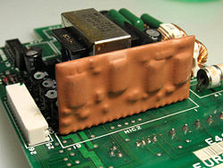
A hybrid integrated circuit, HIC, hybrid microcircuit, or simply hybrid is a miniaturized electronic circuit constructed of individual devices, such as semiconductor devices (e.g. transistors and diodes) and passive components (e.g. resistors, inductors, transformers, and capacitors), bonded to a substrate or printed circuit board (PCB). Hybrid circuits are often encapsulated in epoxy, as shown in the photo. A hybrid circuit serves as a component on a PCB in the same way as a monolithic integrated circuit; the difference between the two types of devices is in how they are constructed and manufactured. The advantage of hybrid circuits is that components which cannot be included in a monolithic IC can be used, e.g., capacitors of large value, wound components, crystals, inductors.
Thick film technology is often used as the interconnecting medium for hybrid integrated circuits. The use of screen printed thick film interconnect provides advantages of versatility over thin film although feature sizes may be larger and deposited resistors wider in tolerance. Multi-layer thick film is a technique for further improvements in integration using a screen printed insulating dielectric to ensure connections between layers are made only where required. One key advantage for the circuit designer is complete freedom in the choice of resistor value in thick film technology. Planar resistors are also screen printed and included in the thick film interconnect design. The composition and dimensions of resistors can be selected to provide desired values. The final resistor value is determined by design and can be adjusted by laser trimming. Once the hybrid circuit is fully populated with components, fine tuning prior to final test may be achieved by active laser trimming.
Some modern hybrid circuit technologies, such as LTCC-substrate hybrids, allow for embedding of components within the layers of a multi-layer substrate in addition to components placed on the surface of the substrate. This technology produces a circuit that is, to some degree, three-dimensional.

- Pre:Thick film technology 2015/12/4
- Next:Characteristics of thick film 2015/12/4

